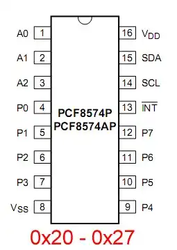
Fig. 1
Programming PCF8574P 8-bit I-O Expander with PICAXE, Arduino
by Lewis Loflin
Also see Connecting PCF8574P GPIO Expander to Raspberry Pi.
I bought 10 PCF8574P GPIO expanders. Each unit has 8 general purpose IO pins each independently programmable. It is controlled through standard I2C 100KHz protocol.
It also includes an open-drain interrupt on change output pin. The voltage range is 2.5V to 6V.
The big problem is the specification sheet - it is terrible. It is hard for the novice to understand. The programming examples on the internet utilize Arduino. While it is easy to write a byte and light 8 LEDs, mixed IO configurations are never explained. Or they utilize some separate mystery library.
I want to know how to program the PCF8574P on multiple controllers - PICAXE and Raspberry Pi. I want to know what the outputs really do to connect more than a few LEDs.
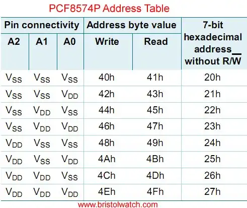
Fig. 1a
Which Address?
Fig. 1 illustrates the pin connections for the PCF8547 and PCF8475P. Fig. 1a address pin connections. First problem is the spec sheet is confusing on the I2C device address. Each device has single byte address with no data direction register (DDR). The three address pins (A0-A2) allow the use of 8 separate devices on a single I2C buss. This is a total 64 individual IO pins.
To quote:
The PCF8574 and PCF8574A are functionally the same, but have a different fixed portion (A6 to A3) of the slave address. This allows eight of the PCF8574 and eight of the PCF8574A to be on the same I2C-bus without address conflict.
Spec sheet table 4 PCH8475 address as 20H to 27H. Yet table 5 specified PCF8574A as 38H to 3FH. Fig.1 above was taken from the spec sheet for the PCF8475P-PCF8475AP - there was no table for those!
Turned out the PCF8475P was the same as the PCF8475 in table 4. What a mess. I found this out testing the device.
One could use 8 PCF8475s and 8 PCF8475As on the same I2c buss for 128 independent IO pins.
To quote:
The PCF8574 and PCF8574A are identical, except for the different fixed portion of the slave address. The three hardware address pins allow eight of each device to be on the same I2C-bus, so there can be up to 16 of these I/O expanders PCF8574/74A together on the same I2C-bus, supporting up to 128I/Os (for example, 128LEDs).
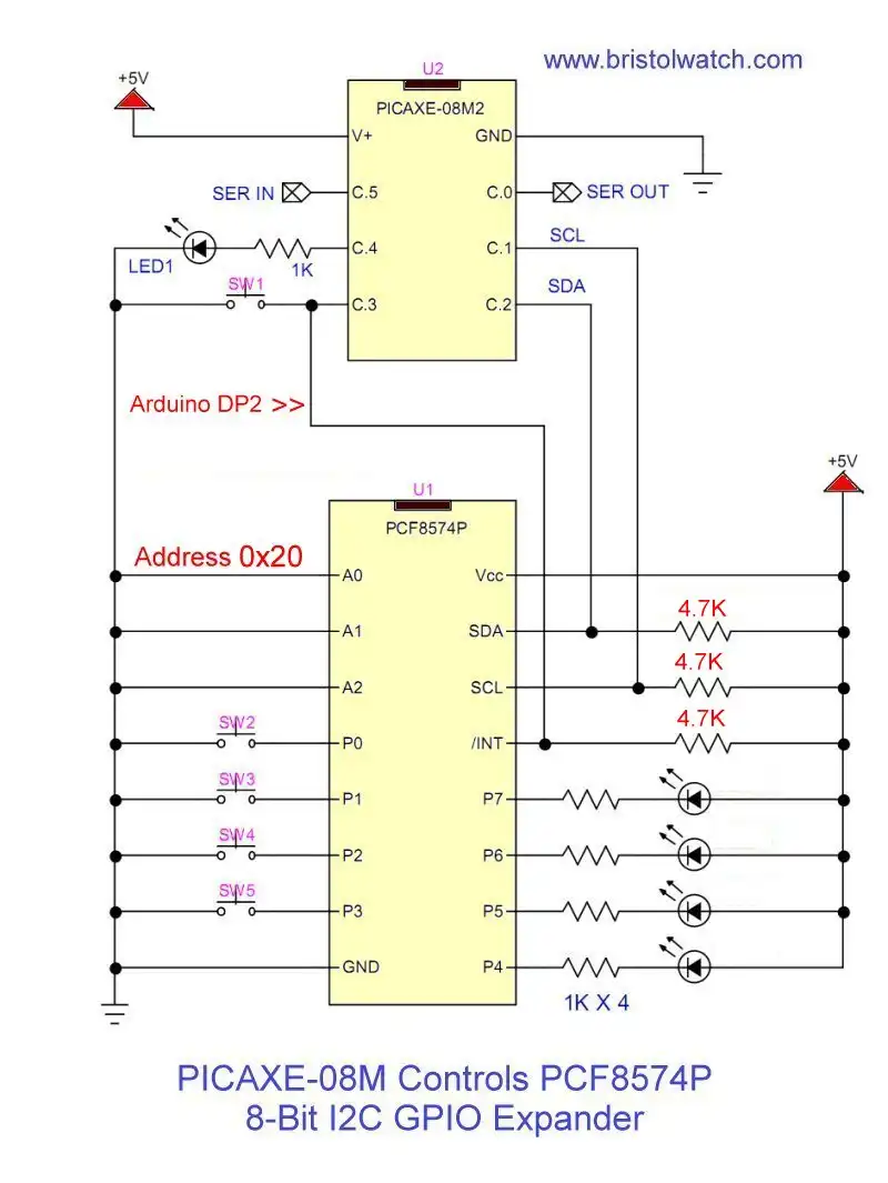
Fig. 2
Quasi-bidirectional I/Os?
Not really a mess but again confusing.
This does not operate in the same manner as an IO pin on say Arduino. On an Arduino, PICAXE, etc. we can connect an LED (observe polarity) through a resistor to either ground or +Vcc.
There is no data direction register (DDR) and this allows a single address. In my case I grounded A0-A2 and used address 0x20 shifted left 1-bit to 0x40.
While the PCF8475 IO can sink 20mA (LEDs 2-5 in Fig. 2) it can not source an LED such as LED1 in Fig. 2. A HIGH out is only a 100uA pull up! This barely turns on an LED even with no resistor.
To program a pin as an input write a binary 1. This turns on the pull up. Then read the bit for HIGH or LOW. A LOW is generated by for example a switch connected to ground. External pull up resistors are not required.
The only output is writing a binary 0 switching an internal transistor to ground sinking the current. I used an LED connected to +Vcc through a 1K resistor.
Sample Program
A PICAXE microcontroller is a Microchip PIC programmed with a basic interpreter. Not as sophisticated as Arduino it is easier to set up and use.
PICAXE basic is closer to the underlying hardware. It also has several outstanding commands such as "button" for interfacing switches.
The downside for some is more knowledge of hardware is required. But it requires no external parts such as a crystal. Clock speed is selectable up to 32mHz.
The default frequency is 4mHz. If using a higher frequency "pause", etc. timing will change.
I2C is set up for 0x40. With PICAXE I2C the address must be shifted one bit left. So 0x20 becomes 0x40, etc.
This is not done with Arduino I2C.
This program "polls" the PCF8574P interrupt pin indicating a switch (SW1-SW5) has been pressed. Separate switch SW1 input is also connected the interrupt pin.
If any switch is pressed pin C.3 (symbol SW1) goes LOW.
The "button" command does debouncing, etc. The PCF8574 interrupt is interrupt on change - LOW to HIGH generates an interrupt, then the HIGH to LOW generates an interrupt. This is true be it SW1 or PCF8574 INT pin.
This is not a true interrupt.
A read is performed on the PCF8574 with the value returned in temp1.
The value in temp1 is shifted 4 places left then 16 (0x0F) is added, stored in temp2. A PICAXE-08M2 has no left-right shift commands but multiplying-dividing by powers of 2 does the same thing.
Then temp2 is written back the the PCF8574. The "toggle LED1" inverts the state of LED1. This is merely a key press indicator.
What this does is "toggle" the state of LEDs on P4-P7 based on the associated switch SW2-SW5.
Remember this is a interrupt on change! There is an interrupt when I press the switch, there is an interrupt when I release the switch.
When SW1 is pressed the LEDs are all turned off.
Arduino Demo 1
Counts from 0 to 16 on LEDs on P4-P7. The value of "i" is shifted four places left, XORed to invert the bits, then written to the PCF8574.
#picaxe 08m2 ; type chip used
; 36 bytes of 2048
;PCF8574P base address 0x20
; shift 1 bit left to 0x40

symbol Int_In = C.3
symbol temp1 = B0
symbol temp2 = B1
symbol temp3 = B2

; set up I2C
hi2csetup i2cmaster, 0x40, i2cslow, i2cbyte

hi2cout 0, (0xFF) ; LEDs off P0-P3 input

main:
; loop back to main if SW1 = HIGH
button Int_In, 0, 200, 100, temp3, 0, main

hi2cin (temp1) ; read PCF8574P
pause 300 ; delay 300mS
temp2 = temp1 * 16 + 0x0F
hi2cout (temp2); send value to PCF8574P

goto main
Arduino Demo 2
This does the same thing as the PICAXE demo above. Notice the code differences. SW1 (interrupt pin) is connected to digital pin 2 on Arduino.
Remember again this is a interrupt on change! There is an interrupt when I press the switch, there is an interrupt when I release the switch. The 300mS delay is there for that reason.
The serial.print commands were used for debugging and can be deleted.
#define SW1 2
#include <Wire.h>
byte temp1, temp2;

void setup()   {
  Wire.begin();
  pinMode(SW1, INPUT);
  Serial.begin(9600);
  Wire.beginTransmission(0x20);
  Wire.write(0xFF);
  Wire.endTransmission();
}  // end setup

void loop() {
  // wait keypress
  while (digitalRead(SW1) == 1) {}
  Wire.requestFrom(0x20, 1);
  temp1 = Wire.read();
  Serial.print(temp1, HEX);
  Serial.print("\n");
  delay(300);
  temp2 = temp1 << 4 | B00001111;
  Serial.print(temp2, HEX);
  Serial.print("\n");
  Wire.beginTransmission(0x20);
  Wire.write(temp2);
  Wire.endTransmission();
} // end loop

- MOSFET-Transistor Drivers with TC4420 and TC4429, IGBTs, etc.
- Introduction TC4420-TC4429 MOSFET Drivers
- Use TC4420 MOSFET Driver for Simple H-Bridge Circuit
- TC4420 MOSFET Driver Various Circuits
- TC4420 MOSFET Driver Replacement Circuits
- Test Power MOSFET Transistors, IGBTs
- Insulated Gate Bipolar Transistor IGBT Circuits
- Issues on Connecting MOSFETs in Parallel
- TC4420 MOSFET Driver Replacement Circuits
- TB6600 Stepper Motor Driver with Arduino
- Interfacing Microcontrollers to CMOS and MOSFET Circuits
- Simplified CMOS-MOSFET H-Bridge Circuit
- Tri-State H-Bridge using CD4093B CMOS Circuit
- Common Collector Opto-Isolated Bipolar Transistor Switches
- Compare 2N3055 MJE10005 Transistor Power Switches
- Connecting PCF8574P GPIO Expander to Raspberry Pi
- Programming PCF8574P 8-bit I-O Expander with Arduino
- DS1307 RTC with a CD4040 as a Precision Time Base
- CD4040 12-stage Binary Counter with DS1307 RTC Time Base
- Pt. 1 Interfacing Microcontrollers to CMOS and MOSFET Circuits
- Pt. 2 Simplified CMOS-MOSFET H-Bridge Circuit
- Pt. 3 Tri-State H-Bridge using CD4093B CMOS Circuit
- Pt. 1 TB6600 Stepper Motor Driver with Arduino
- Pt. 2 Program TB6600 Stepper Motor Driver with Arduino
- TB6600 Stepper Motor Driver with Arduino
- Off Site:
- Web Master
- Tri-Cities VA-TN
- General Science
- Hobby Electronics
- US Constitution
- Christianity 101
- Religious Themes
© Copyright 2018 Lewis Loflin E-Mail