Fig. 1
SR Latch Microcontroller I-O Pin Tutorial
by Lewis Loflin
Other than voltage-current levels a CMOS OR, NOR, AND, NAND, XOR gates operate identically to their TTL cousins. Note: CMOS and TTL can't be directly connected to each other unless the same voltage without some form of level translation circuits. I'll be addressing that issue in other pages..
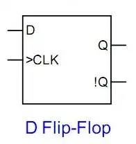
Fig. 2
In my pages Tutorial NOR Gate SR Latch Circuits and Tutorial NAND Gate SR Latch Circuit I introduce how to use SN74LS02 NAND gates and SN74LS00 NAND gates respectively construct a basic digital flip-flop, SR latch, and D-flip-flop.
The above circuit in Fig. 2 is built from NAND or NOR gates. It's also called a one-bit data latch. While the internal construction differs the function is identical: store one bit of data when the voltage on the CLK pin changes.
If the Q output is HIGH then the !Q output is LOW and vice-versa. It will remember the last condition until changed or power is removed.
These flip-flop type circuits are the basis of all modern computers and micro-controllers. Modern micro-controllers have internal memory often flash for program storage, EEPROM, and static scratchpad RAM. Some require an external oscillator crystal.
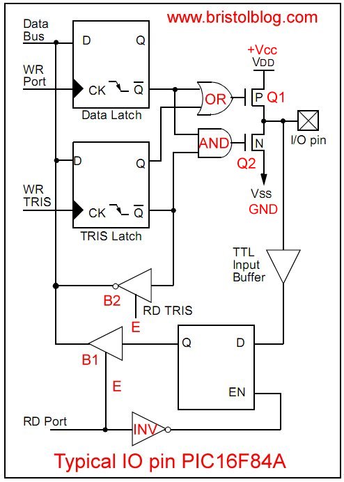
All have programmable Input-Output pins. Fig. 1 illustrates a single I/O pin on a Microchip PIC16F84A. By writing binary data to specific static memory locations we setup hardware modules and configuration of the I/O pins.
Microchip PIC which stands for Peripheral Interface Controller have many variations from basic to super powerful. Can also be programmed in C or assembly through software known as MPLAB from Microchip.
Positive: price and flexibility.
Negatives: must be compiled and uploaded through a separate PIC programmer. The C in MPLAB is copyrighted (I think). I never use C on basic low end devices. I use assembly for that.
Assembly requires a lot of knowledge of the particular controller along with electronics. Not for beginners.
It uses three D-flip-flops similar to those constructed from NAND and NOR gates. Q1 and Q2 are MOSFETs or metal-oxide field effect transistors. They are voltage operated and in this case can "source" or "sink" 25 milliamps (mA) or 0.025 amps.
The configuration is known as Tri-State. The I/O pin can be HIGH, LOW, or floating (Hi-Z).
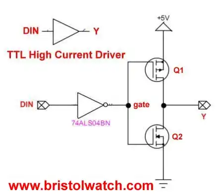
Fig. 3
While this is connected in a Tri-State configuration the following webpage introduces this circuit as a non-tri-state power driver or buffer circuit in Fig. 3. It also illustrates the concept of sink-source connections.
Know the concepts of sink and source!
See High current TTL Driver-Buffer Circuits.
As a quick note I'll assume a 5-volt circuit. A HIGH or binary 1 is 5-volts, a LOW or binary 0 is 0-volts. Current flow is assumed to be from positive to negative.
Also see the following on MOSFET transistor switches. Yes there are two basic types that differ by direction of current flow.
- Exploring Solid State Relays and Control Circuits
- Comparing Photo Triac, Photo SCR Opto-Couplers
- Light Activated SCR Based Optocouplers Circuit Examples
- Silicon Controlled Rectifier Review and Circuits
- Silicon Controlled Rectifiers Connected as Power Triacs
- Insulated Gate Bipolar Transistor IGBT Circuits
- Current Limiter Circuits for Opto-Coupler LEDs
- VOM1271 Photovoltaic MOSFET Driver Circuits
- Current Limiter Allows Safe Testing of Zener Diodes, LEDs
- 3 Amp LM741 Op-Amp Constant Current Source
- Bidirectional Solid State Relay Circuits
- Simple Solid State Relay for Low Power LED 120V Lamps
- Build High Power MOSFET Directional Switch Relay
- Optical Isolation of H-Bridge Motor Controls
- All NPN Transistor H-Bridge Motor Control
- Basic Transistor Driver Circuits for Micro-Controllers
- ULN2003A Darlington Transistor Array with Circuit Examples
- Tutorial Using TIP120 and TIP125 Power Darlington Transistors
- Driving 2N3055-MJ2955 Power Transistors with Darlington Transistors
- Understanding Bipolar Transistor Switches
- N-Channel Power MOSFET Switching Tutorial
- P-Channel Power MOSFET Switch Tutorial
- Build a Transistor H-Bridge Motor Control
- H-Bridge Motor Control with Power MOSFETS
- More Power MOSFET H-Bridge Circuit Examples
- Build a High Power Transistor H-Bridge Motor Control
- H-Bridge Motor Control with Power MOSFETS Updated
- Opto-Isolated Transistor Drivers for Micro-Controllers
- Comparator Theory Circuits Tutorial
- Constant Current Circuits with the LM334
- LM334 CCS Circuits with Thermistors, Photocells
- LM317 Constant Current Source Circuits
- TA8050P H-Bridge Motor Control
- All NPN Transistor H-Bridge Motor Control
- Basic Triacs and SCRs
- Comparator Hysteresis and Schmitt Triggers
- Comparator Theory Circuits Tutorial
- Photodiode Circuits Operation and Uses
- Optocoupler MOSFET DC Relays Using Photovoltaic drivers
- Connecting Crydom MOSFET Solid State Relays
- Photodiode Op-Amp Circuits Tutorial
- Optocoupler Input Circuits for PLC
- H11L1, 6N137A, FED8183, TLP2662 Digital Output Optocouplers
- Optical Isolation of H-Bridge Motor Controls
- All NPN Transistor H-Bridge Motor Control
© Copyright 2019 Lewis Loflin E-Mail