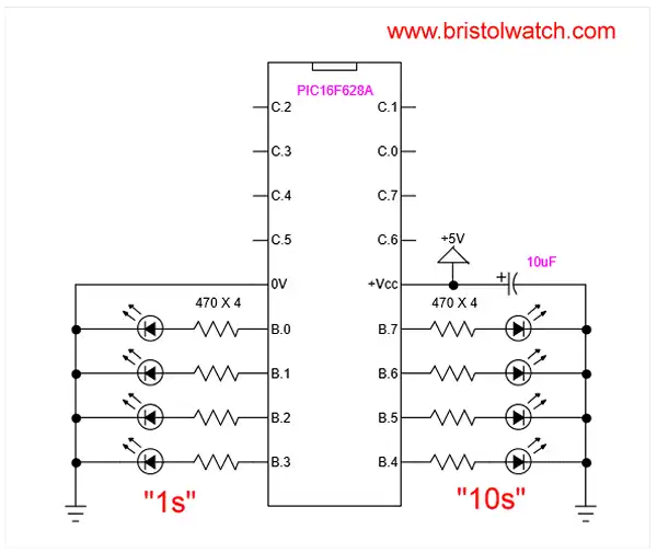
PIC16F628A Test Setup.
Fig. 1
Click here for larger image.


Setup PIC16F628A Pulse-Width-Modulation

by Lewis Loflin


Setup for PWM output. Make sure RB3 is 0 (output) in TRISB.


        ; Calculate PWM values:
	; www.micro-examples.com PWM Calculator.
	; PR2 = %11111001 'Timer2 Module Period Register - Bank 1
	; rest bank 0
	; T2CON = %00000101  
	; P52, Bits 6-3 postscaler, 0000 = 1:1
	; Bit 2 TMR2ON, 1 = ON, 0 = OFF
	; Bits 1-0 prescaler value 01 = 1:4
	; CCPR1L = %0  ' duty cycle 0-255
	; CCP1CON = %00001100  'CCP1 control register 
	; Buts 3-0 CCP mode select, 110x =  PWM active high
	; Bits 5-4 PWM LSB
	; Bits 7-6 unused
	
	BANKSEL 1 ; Bank 1
	MOVLW B'11111001'
	MOVWF PR2
	BANKSEL 0 ; Back Bank 0
	MOVLW B'00000101'
	MOVWF T2CON
	MOVLW 0 ; duty cycle
	MOVWF  CCPR1L ; duty cycle 0-255
	MOVLW B'00001100'
	MOVWF CCP1CON  

Instead of writing 0 value to PWM counters to turn off the output we simply change the IO pin RB3 to input with TRISB bit RB3 in bank 1.

Download the ASM code 16F628A_PWM.asm.

See How I got into Electronics


;*********************************************  
; Filename: 16F628A_PWM.asm 
; Uses PIC16F628A
; Date: 13 Nov. 2013      
; Author:  Lewis Loflin
; http://www.bristolwatch.com
; http://www.bristolwatch.com/PIC16F628A/a7.htm
; Delay routines based on 4 mHz Fosc / 4 = 1uSec.
; LED1 on RB1 blinks 1Hz, PWM LED on RB3 off to bright to off.
; PWM output PORTB, 3 
;*******************************************

list      p=16f628A           ; list directive to define processor
#include <p16F628A.inc>       ; processor specific variable definitions
errorlevel  -302              ; suppress message 302 from list file

__CONFIG _CP_OFF & _LVP_OFF & _BOREN_OFF & _MCLRE_OFF & _WDT_OFF & _PWRTE_ON & _XT_OSC 
	
; Use  _FOSC_INTOSCIO  for
; Internal 4 mHz osc and no ext reset, MCLR pin RA5 is input only.
; Internal RC OSC PCON bit 3 must be set
; 1 = 4mHz, 0 = 38 kHZ

; Use _HS_OSC for a 16 mHz ext crystal.
; Use _XT_OSC for 4 mHz ext crystal. Page 95 in spec sheet. 


;-------------------------- counters	
;*****[ Data Storage Reg's ]*****
	; Assign each reg. from Bank 0 RAM area.
	; total 96 bytes from 0x20 - 0x7F
	CBLOCK  0x20 
	B0
	B1
	B2
	temp1
	temp2
	CNT1
	CNT2
	CNT3
	CNT4
	ENDC ; Conclude Bank 0 RAM assignments.


	ORG     0x000             ; processor reset vector
	goto    setup             ; go to beginning of program

setup ; init PIC16F628A

;************************************************************
	; https://www.micro-examples.com/public/microex-navig/doc/097-pwm-calculator
	; PR2 = %11111001 'Timer2 Module Period Register - Bank 1
	; rest bank 0
	; T2CON = %00000101  
	; P52, Bits 6-3 postscaler, 0000 = 1:1
	; Bit 2 TMR2ON, 1 = ON, 0 = OFF
	; Bits 1-0 prescaler value 01 = 1:4
	; CCPR1L = %0  ' duty cycle 0-255
	; CCP1CON = %00001100  'CCP1 control register 
	; Buts 3-0 CCP mode select, 110x =  PWM active high
	; Bits 5-4 PWM LSB
	; Bits 7-6 unused
	
	BANKSEL 1 ; Bank 1
	MOVLW B'11111001'
	MOVWF PR2
	BANKSEL 0 ; Back Bank 0
	MOVLW B'00000101'
	MOVWF T2CON
	MOVLW 0 ; duty cycle
	MOVWF  CCPR1L ; duty cycle 0-255
	MOVLW B'00001100'
	MOVWF CCP1CON  
	
;*************************************************************
	; Setup TRIS DDR register and PCON register.
	BANKSEL OPTION_REG          ; Switch to Bank 1.
	MOVLW b'111111' ; input
	MOVWF TRISA ;
	MOVLW B'11110001'
	MOVWF TRISB 
	; Setup PCON bit 3, 
	; 1 = 4mHz, 0 = 48kHz
	MOVLW b'00001000'
	MOVWF PCON
	
	
	BANKSEL PORTB  ; Switch to Bank 0.
	MOVLW   0x07  ; comp off
	MOVWF   CMCON  
	CLRF    PORTB  	   

	goto main

main
; remaining code goes here


; Demo 2
; CCPR1L is 8-bit PWM duty cycle reg. 0-255.
; RB3 is PWM output to LED2 to GRD.
; LED2 on pin RB3 goes from off to bright in steps.
; Clear PWM register CCPR1L, LED2 = OFF
; Flip state of LED1 RB1 with XORWF
; W = 50, call delay Wx10ms = 500mSec. 
; 2 loops = 1 Hz. rate on LED1 RB1
; Every loop 20 ADDed to CCPR1L reg.
; LED2 gets brighter
; Every 1Hz 40 is ADDed to PWM CCPR1L
; Check STATUS bit C
; Exit loop if C = 1, C = 0 back aa
; Repeat until STATUS C bit = 1.
	clrf 	CCPR1L
aa	movlw 0x02
	xorwf PORTB, f
	movwf d'50' 
	call Wx10ms ; LED ON 0.5 sec.
	movlw d'20'
	addwf CCPR1L, f
	btfss STATUS, C ; check carry
	goto aa

; CCPR1L is 8-bit PWM duty cycle reg. 0-255.	
; RB3 is PWM output to LED2 to GRD.
; LED2 on pin RB3 goes from bright to off in steps.
; PWM register CCPR1L = 255, LED2 on RB3 is bright
; Flip state of LED1 RB1 with XORWF
; W = 50, call delay Wx10ms = 500mSec. 
; 2 loops = 1 Hz. rate on LED1 on RB1
; Every loop 20 SUBed from PWM CCPR1L reg.
; LED2 get dimmer
; Every 1Hz 40 is SUBed from PWM CCPR1L
; Check STATUS bit C for borrow
; Exit loop if C = 0, C = 1 back  bb
; Repeat until STATUS C bit = 0.
	movlw d'255'
	movwf CCPR1L
bb	movlw 0x02
	xorwf PORTB, f
	movwf d'50' 
	call Wx10ms ; LED ON 0.5 sec.
	movlw d'20'
	subwf CCPR1L, f
	btfsc STATUS, C ; check borrow
	goto bb	
	
	goto	main 

;**************************	;Delay routine.
; Calculating a 1mSec delay. 4mHz is divided by 4
; At 4mHz / 4 = 1uSec. ;  1uSec. * 1000 = 1 mSec.
; GOTO uses 2 cycles, DECFSZ 1 cycle = 3 cycles or 3uSec.
; 3 * ~80 * 4 = ~ 1000uSec. or 1mSec.

delay1ms
	; 4 mhz crystal
	movlw d'4'
	movwf CNT1
	movlw d'80' ; adjust for 500Hz test
	movwf CNT2
	decfsz CNT2, f
	goto $-1 ; 
	decfsz CNT1, f
	goto $-5 
	return

delay10ms
	movlw d'10'
	goto $+2
Wx1ms	; W * 1mSec.
	movwf CNT3
	call delay1ms
	decfsz CNT3, f
	goto $-2
	return

Wx10ms	; W * 10mSec.
	movwf CNT4
	call delay10ms
	decfsz CNT4, f
	goto $-2
	return

	END  ; directive 'end of program'

Bristolwatch.com banner.

Web site Copyright Lewis Loflin, All rights reserved.
If using this material on another site, please provide a link back to my site.